

Research on the third-generation semiconductor SiC industry chain and market applications
I. Overview of Third-Generation Semiconductors
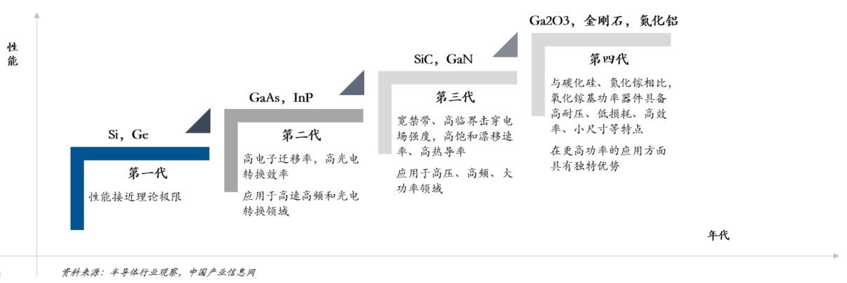
SiC exhibits significant advantages over Si in terms of physical properties. Coupled with the major transformation in energy conservation, emission reduction, and the new energy sector, the downstream applications of SiC are extremely broad. Most existing power devices are based on silicon semiconductor materials. Due to the limitations of silicon's physical properties, the energy efficiency and performance of devices have gradually approached their limits, making it difficult to meet the rapidly growing and changing needs of new power applications. Silicon carbide power devices, with their excellent high-voltage, high-temperature, and low-loss properties, can effectively meet the requirements of high efficiency, miniaturization, and lightweight design in power electronic systems. They have clear advantages in new energy vehicles, photovoltaic power generation, rail transit, and smart grids.
II. Silicon Carbide Industry Chain Analysis
1. Overview of the Silicon Carbide Industry Chain
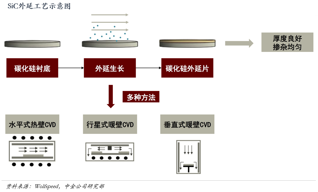
The SiC industry chain mainly includes substrate, epitaxy, device manufacturing, and packaging and testing. In SiC substrate manufacturing, carbon powder and silicon powder are first reacted at high temperatures to obtain high-purity SiC fine powder, which is then placed in a single-crystal growth furnace for high-temperature sublimation to form SiC crystals. Finally, the SiC crystals are processed into SiC substrates through ingot processing, cutting, grinding, polishing, and cleaning. Depending on the substrate resistivity, SiC substrates can be classified as conductive or semi-insulating substrates. Because the substrates have some defects, they are not suitable for direct semiconductor device manufacturing, so a layer of high-quality epitaxial material is usually deposited on the substrate.
Conductive SiC substrates typically have another layer of SiC epitaxially grown on them for the fabrication of power devices. These are suitable for high-temperature and high-voltage operating environments and offer low losses, mainly used in power electronics such as inverters, converters, motor drivers, and onboard chargers in new energy vehicles; diodes, inverters, and converters in photovoltaic power generation; traction converters, auxiliary converters, integrated main and auxiliary converters, power electronic transformers, and power chargers in rail transit; and high-voltage direct current transmission converters, flexible direct current transmission converters, flexible alternating current transmission devices, high-voltage direct current circuit breakers, and power electronic transformers in smart grids. Semi-insulating SiC substrates can have GaN material epitaxially grown on them for the fabrication of radio frequency devices. These are suitable for high-frequency and high-temperature operating environments and are mainly used in the radio frequency field such as power amplifiers in 5G communication and radio detectors in defense applications.

2. Silicon Carbide Crystal Growth
The principle of the PVT method is to place the raw materials in a high-temperature zone and the seed crystal in a relatively low-temperature zone. The raw materials in the higher temperature zone decompose and directly produce gaseous substances without passing through a liquid phase. These gaseous substances are transported to the seed crystal under the drive of the axial temperature gradient, where they nucleate, grow, and crystallize to form silicon carbide single crystals. The main technical challenges faced by the PVT method are twofold: one is the control of impurity concentration in silicon carbide crystals, including re-purification of graphite materials and the acquisition of high-purity silicon carbide fine powder raw materials; and the second is the unreasonable temperature distribution inside the crucible, which may lead to defects such as micro-pipes and dislocations. Because the key graphite components used in the PVT method for growing silicon carbide crystals can be reused more than 20 times, it significantly reduces the cost of silicon carbide crystal growth and is currently the mainstream method for SiC crystal growth. Currently, foreign companies such as Cree, II-VI, SiCrystal, Dow, and domestic companies such as Tianyue Advanced and Tianke Heda all use this method.
The principle is to introduce high-purity gases such as silane, ethane, propane, or hydrogen at a high temperature of 1500-2500°C and allow them to react in the growth chamber. A silicon carbide precursor is first formed in the high-temperature zone and then transported by gas to the seed crystal end in the low-temperature zone for deposition to form a single crystal. The main technical challenge faced by the HTCVD method is the control of the deposition temperature. Studies have shown that excessively high deposition temperatures are accompanied by excessively fast deposition rates, leading to a loose crystal structure, while excessively low deposition temperatures are accompanied by excessively slow deposition rates, leading to a porous structure. The HTCVD method produces crystals with higher purity and allows for near-uniform crystal growth, but the gaseous substances can react with the crucible causing fluctuations in the gas phase composition, affecting the quality of the grown crystals, and the crystal growth cost is higher. Currently, foreign companies such as Norstel and Denso Corporation use this method.
The principle is to dissolve carbon from the high-temperature part at the bottom of the crucible into the silicon melt in the graphite crucible, and allow the silicon carbide seed crystal to contact this carbon-silicon melt for epitaxial growth to obtain a silicon carbide single crystal. The main technical challenge of the LPE method is the selection of transition metals. The solubility of carbon in silicon solution is too low, so transition metal elements must be added to the silicon melt to increase the carbon concentration and improve the crystal growth rate. Crystals grown using the LPE method exhibit high quality and low defect density, meeting the requirements for the preparation of high-quality silicon carbide single crystals, but the growth rate is slow, and the growth length is also limited. Currently, Sumitomo Metal Mining Co., Ltd. uses the LPE method.
3. Silicon Carbide Substrate Preparation
According to the China Association for Science and Technology, citing Future Think Tank, taking the mainstream PVT method as an example, SiC substrate preparation faces the following challenges:
Difficult Temperature Control: Taking the mainstream Physical Vapor Transport (PVT) method as an example, SiC ingots require production at 2500℃, while silicon crystals only need 1500℃. This necessitates specialized single-crystal furnaces and precise control of growth temperature during production, making it extremely challenging.
High Requirements for Product Parameters, Difficult Real-time Control of Black Box Yield: Core parameters of SiC wafers include micro-pipe density, dislocation density, resistivity, warpage, surface roughness, etc. During crystal growth, the silicon-carbon ratio, temperature gradient, crystal growth rate, and gas flow pressure must be precisely controlled; otherwise, polycrystalline inclusions are easily generated, resulting in unqualified crystals. The inability to directly observe crystal growth within the graphite crucible (a 'black box') requires extremely precise thermal field control, material matching, and accumulated experience.
Difficult Crystal Diameter Increase: Under the physical vapor transport method, increasing the diameter of SiC crystals is extremely difficult, with the difficulty increasing exponentially as the crystal size increases.
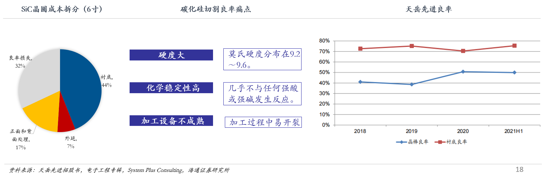
Generally Low Yield: Low yield is mainly due to two stages: (1) Ingot yield = (Semiconductor-grade ingot output / (Semiconductor-grade ingot output + Non-semiconductor-grade ingot output)) × 100%; (2) Substrate yield = (Qualified substrate output / (Qualified substrate output + Unqualified substrate output)) × 100%.
4. Silicon Carbide Epitaxy
5. Silicon Carbide Devices
Silicon-based power semiconductors are mainly MOSFETs and IGBTs, with discrete devices and modules accounting for a combined 45% and maintaining long-term stability. The combined market size of discrete devices and modules (including IGBT modules and IPM intelligent modules) is approximately $18 billion, with MOSFETs and IGBTs accounting for the largest share, with market sizes of $7.4 billion and $5.4 billion, respectively. IGBTs can be further divided into discrete devices, modules, and IPMs.
The mainstream forms of silicon carbide devices (single tubes) are diodes and MOSFETs, with a growing variety of module products.
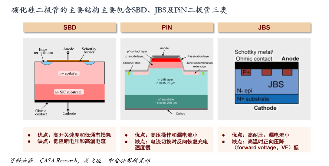
Diodes: Silicon carbide diodes mainly include Schottky barrier diodes (SBD), junction barrier Schottky diodes (JBS), and PiN diodes (PND type). In terms of device structure, silicon carbide has no innovation compared to silicon-based devices, but the excellent properties of the material give silicon carbide products a competitive advantage. Specifically: 1) SiC SBDs have high withstand voltage and almost no reverse recovery time, which can significantly reduce switching losses, increase switching frequency, and greatly optimize the performance of diodes in the 200V-1700V voltage range, and shift the application sweet spot of PiN to above 3300V; 2) For higher-end JBS devices, SiC JBS has the advantages of high current density and high operating junction temperature, with further performance improvements compared to silicon-based devices.
6. Silicon Carbide Device Manufacturing
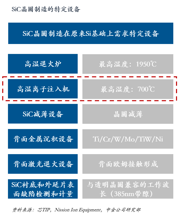
Most of the equipment for manufacturing silicon carbide devices is the same as that used for traditional silicon production. However, due to the high hardness and melting point of silicon carbide, some special production equipment and processes are required. Specific equipment required for SiC includes high-temperature annealing furnaces, high-temperature ion implanters, SiC thinning equipment, back metal deposition equipment, back laser annealing equipment, and SiC bottoming and epitaxial wafer surface defect detection and measurement equipment.
High-temperature ion implanter (high-temperature, high-dose, high-energy ion implantation process): Silicon devices can be doped using diffusion and ion implantation methods, while silicon carbide devices can only be doped using ion implantation. If the diffusion method is used to dope silicon carbide devices, the required diffusion temperature is much higher than that of silicon. At a high temperature of 1800 degrees, defects will also be generated in the silicon carbide material, so only high-temperature ion implantation can be used to dope silicon carbide. In addition, due to the good stability of SiC, it is difficult to recrystallize, and doping activation is also difficult. Its ion implanter needs to have high temperature and high energy characteristics, and needs more precise control of ion implantation concentration and depth, as well as ion implantation surface protection technology. The technical difficulties lie in ion source technology and high-temperature target chamber technology.
High-temperature annealing furnace (ultra-high-temperature annealing process): Compared with silicon, the temperature of the silicon carbide annealing furnace is higher, at 1600-1700 degrees in argon (Ar), and the equipment requirements are higher. In addition, although high-temperature and long-time annealing can improve the activation rate, high temperature can also cause large undulating defects on the surface of the device, and can also cause the implanted ions to escape from the surface. Therefore, the difficulties of this type of equipment lie in the design of the high-temperature furnace chamber's thermal field and the rapid heating, cooling, and temperature control technology.
High-temperature oxidation furnace (high-quality oxide layer growth process): For MOSFET devices, the gate oxide can directly affect the gate reliability and MOSFET performance. For silicon carbide MOSFETs, if the quality of the SiC-SiO2 interface is low, it will reduce the channel mobility and lead to unstable threshold voltage. Moreover, since silicon and carbon atoms are present in silicon carbide materials, very special gate dielectric growth methods are required. High-temperature oxidation furnaces can generate high-quality gate oxide layers with low interface state density, improve the SiO2/SiC interface, and are necessary special equipment for preparing the gate oxide layers of silicon carbide devices. The operating temperature of high-temperature oxidation furnaces is generally higher than 1350 degrees, the vacuum degree in the furnace tube can be as low as 1 mbar, and the content of metal contaminants in the cavity is extremely low.
7、Silicon Carbide Device Packaging
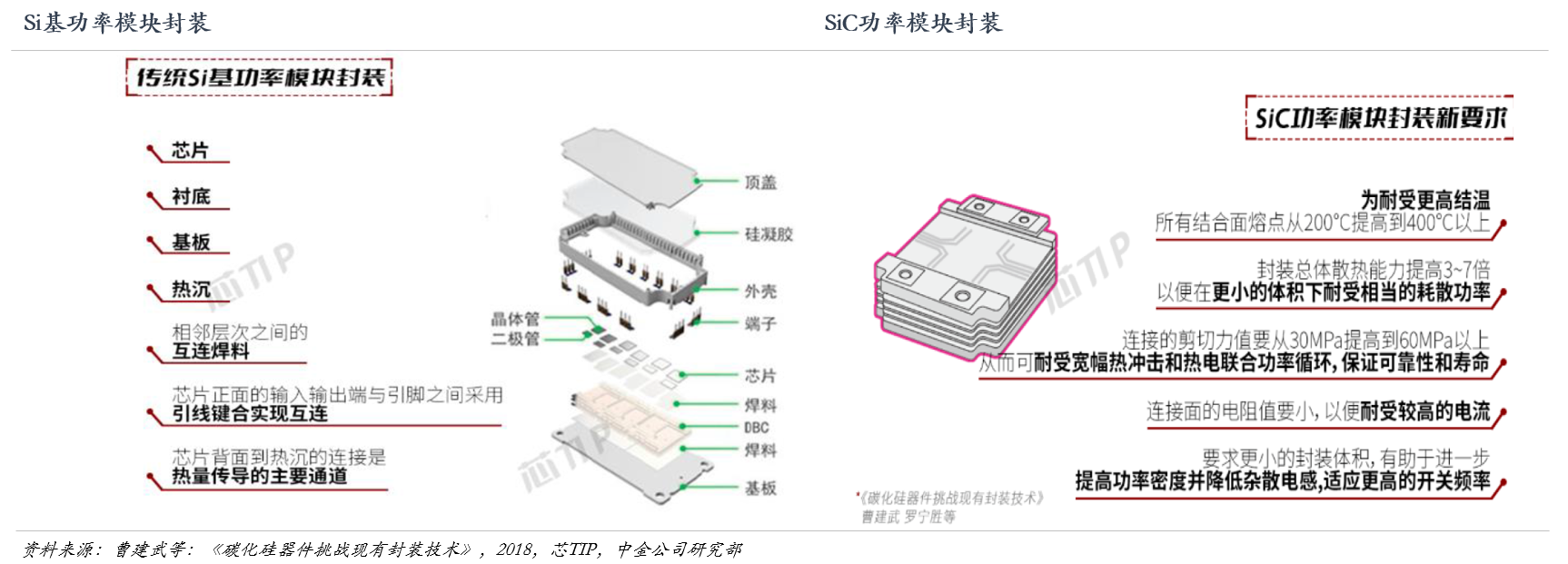
Traditional silicon-based module packaging cannot meet the requirements of silicon carbide module packaging. Traditional silicon devices mostly use wire bonding and single-sided heat dissipation methods, welding the back of the chip to the substrate, using metal bonding wires to lead out the front electrodes, and finally encapsulating or potting. Although this method has low cost and mature technology, it cannot fully meet the needs of silicon carbide MOSFET modules, mainly due to the following two problems:
High parasitic inductance: Due to its high-frequency characteristics, SiC devices can achieve high switching speeds. However, the rate of change of voltage and current during the switching process (dv/dt and di/dt) is extremely large, and parasitic inductance in this case is very easy to cause voltage overshoot and oscillation, leading to increased losses, increased device voltage stress, and electromagnetic interference problems.
Low heat dissipation efficiency: Due to the high temperature resistance of SiC itself, the operating temperature can reach above 300℃, while the packaging of traditional silicon devices can generally only operate below 150℃. In addition, silicon carbide modules have a significantly smaller volume than silicon modules of the same power level, and silicon carbide modules have higher requirements for heat dissipation. When working at high temperatures, silicon carbide devices may also face various problems caused by the mismatch of thermal expansion coefficients of different packaging materials and thermal stress at the interface. Therefore, when manufacturing silicon carbide modules that parallel multiple silicon carbide chips, how to improve the heat dissipation performance of the module in terms of packaging is key.
III. Analysis of Silicon Carbide Application Scenarios
1. Core Commercial Value of Silicon Carbide
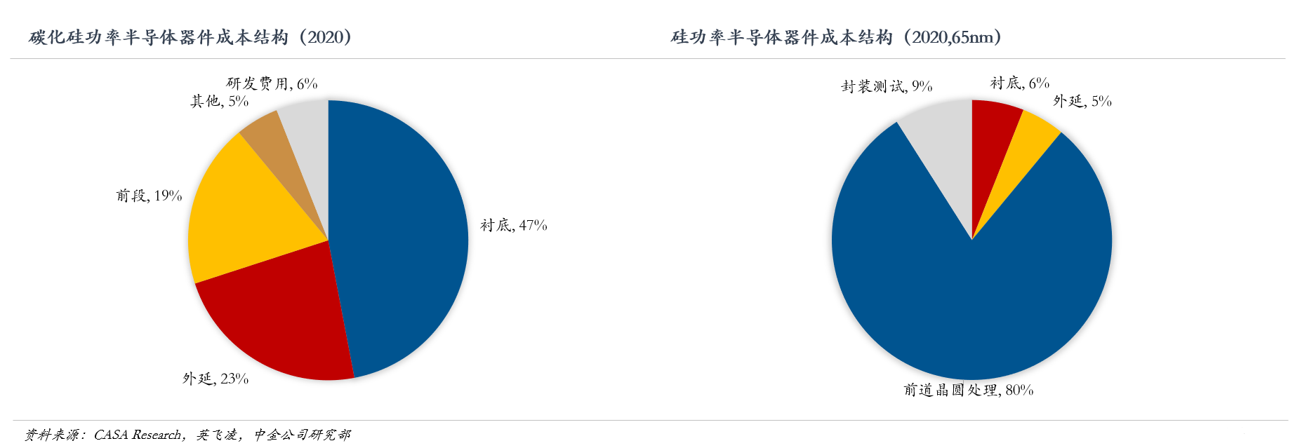
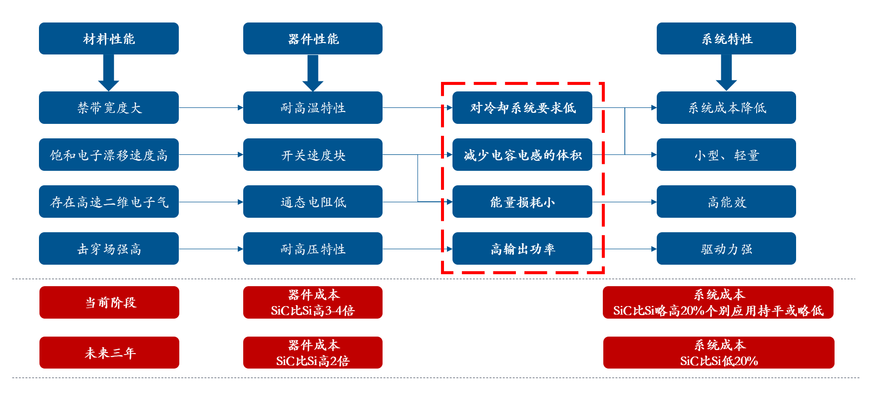
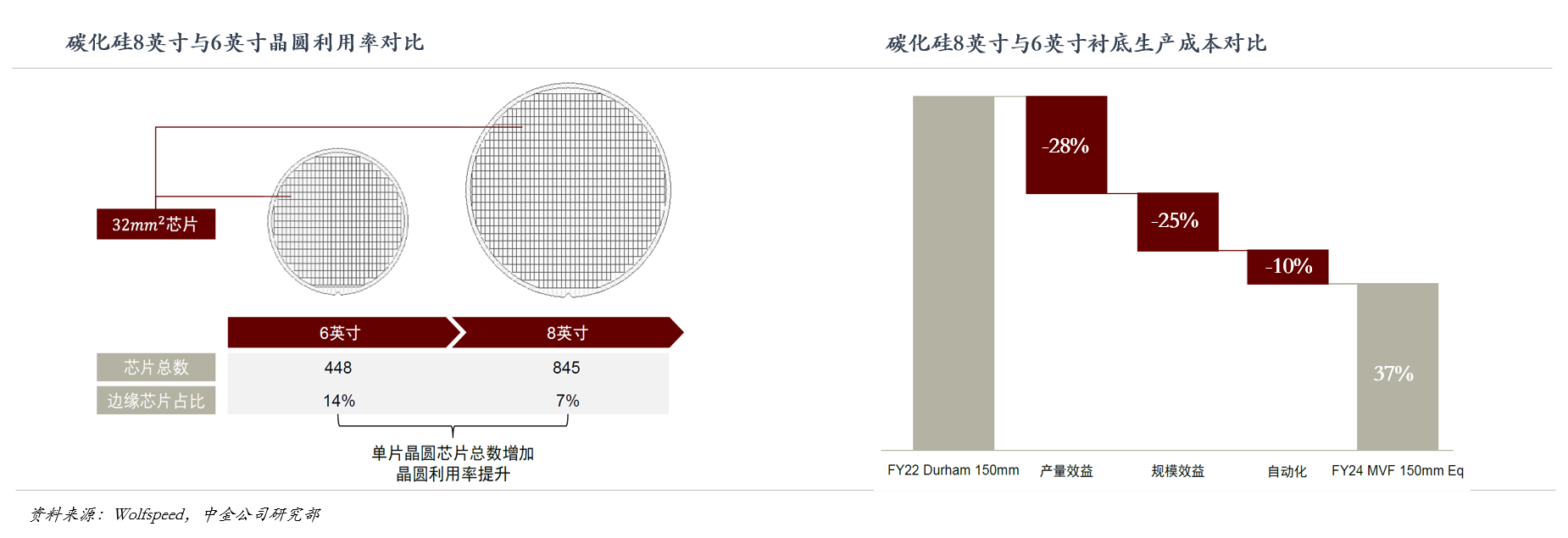
Currently, the core factor inhibiting downstream customers from massively purchasing silicon carbide diodes/MOSFETs to replace silicon diodes/IGBTs is the significant increase in cost. Due to the still relatively low yield and efficiency of silicon carbide substrate manufacturing, and the still relatively high barriers on the device processing and module packaging sides, the current production cost of silicon carbide devices is high, pushing up their prices and causing significant cost pressure on target customers in the market. For example, 1) In terms of diode products, the current price of mainstream SiC diode products is 1.3 times that of Si diodes of the same specification; 2) In terms of MOSFET products compared with IGBT products, the current price of SiC MOSFETs is approximately 3-4 times that of comparable Si IGBT devices.
However, under the premise that the cost of SiC devices is difficult to achieve parity with Si, silicon carbide still has commercial value. The core reason is that the increase in semiconductor cost is exchanged for an increase in system efficiency, which can ultimately lead to a reduction in system cost, or help downstream customers achieve greater economic benefits over the entire life cycle of the product. As the cost of silicon carbide gradually decreases, the downstream market is also expected to experience significant growth.
The increase in the cost of silicon carbide devices is exchanged for an increase in system efficiency, which can ultimately lead to a reduction in system cost.
In recent years, the unit price of semi-insulating and conductive substrates has been decreasing year by year. It is expected that with the gradual implementation of global capacity expansion, the unit price of substrates will continue to decline in the next 3 years, which will help accelerate the overall improvement of the downstream penetration rate of silicon carbide. According to CASA's prediction, with the decline in the prices of SiC upstream substrates and epitaxy, the prices of SiC diodes and SiC MOSFETs are expected to decline at a rate exceeding 10% per year.
2. New Energy Vehicle Field
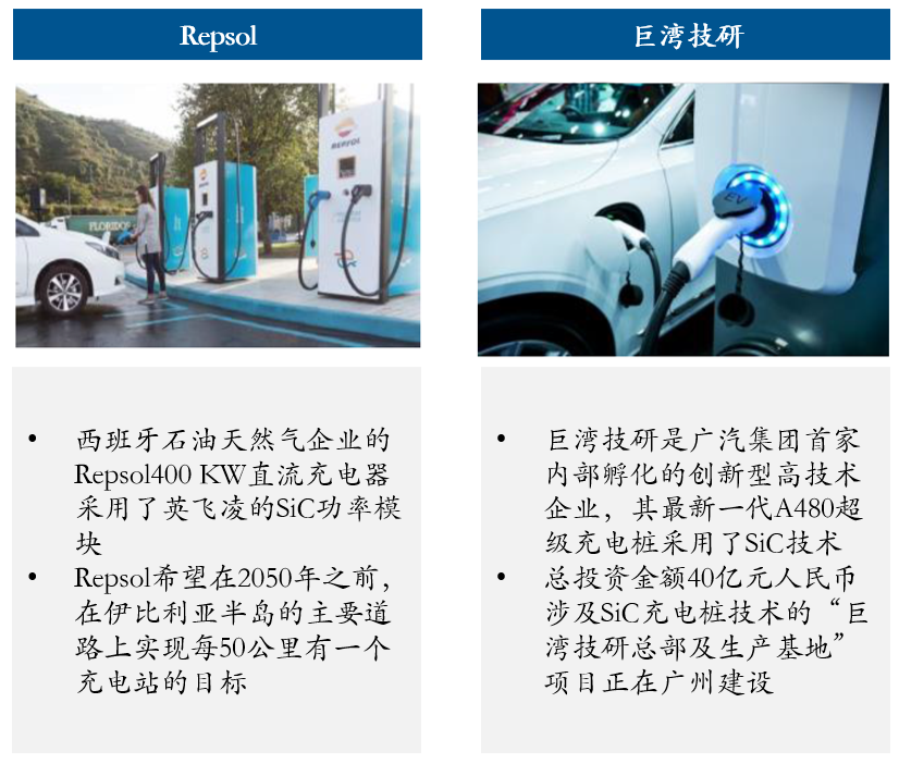
In the field of new energy vehicles, the main applications of SiC are in electric drive inverters, on-board chargers (OBC), and DC-DC converters. According to Wolfspeed's forecast, by 2026, inverter applications will account for more than 80% of the automotive SiC device market, making it the most important application area. SiC devices used in electric drive inverters can significantly reduce the size, weight, and cost of power electronic systems, and improve power density; their application in on-board chargers and DC-DC systems can reduce switching losses, increase the maximum operating temperature, and improve system efficiency. In addition, SiC can also be used in new energy vehicle charging piles to reduce the size of the charging pile and improve charging speed.

(1) New Energy Vehicle Main Inverter
Using SiC devices to replace Si IGBTs with a 450V DC bus voltage, the inverter efficiency is expected to increase by 5%; using an 800V system and a SiC inverter is expected to bring a 7.6% efficiency improvement to the system.
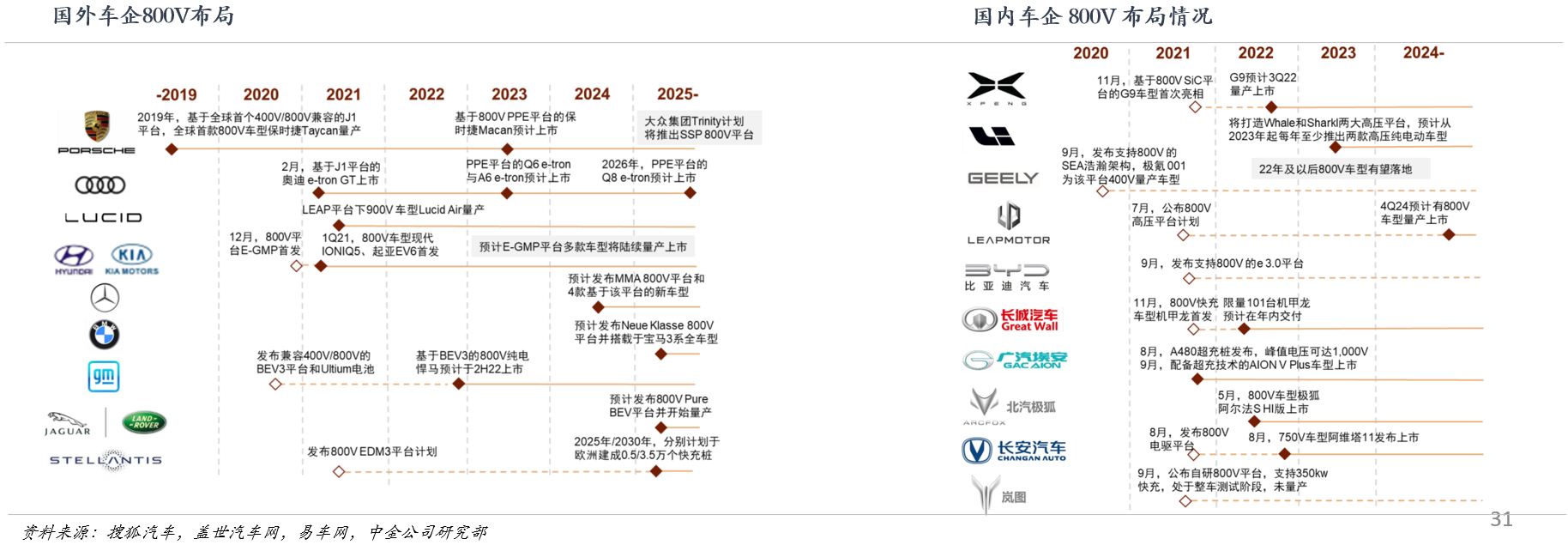
The two major pain points affecting the market scale of electric vehicles are range anxiety and slow charging speed. The high-voltage mode, with its advantages of increasing range and saving space and weight, has become the best solution to solve these two pain points. The voltage platform of electric vehicles is rising to 800V, becoming a trend.
The 800V platform significantly increases the voltage requirements for power devices, and SiC MOSFETs have a greater advantage. Under 800V voltage, the corresponding power device voltage needs to be increased to around 1200V. Currently, 400V models generally use Si IGBT devices, while 800V models need to be upgraded to SiC MOSFETs. Although both Si IGBT and SiC MOSFET can meet the 1200V voltage requirement, SiC MOSFET, based on its material and device structure characteristics, has significant advantages in low loss and high frequency.
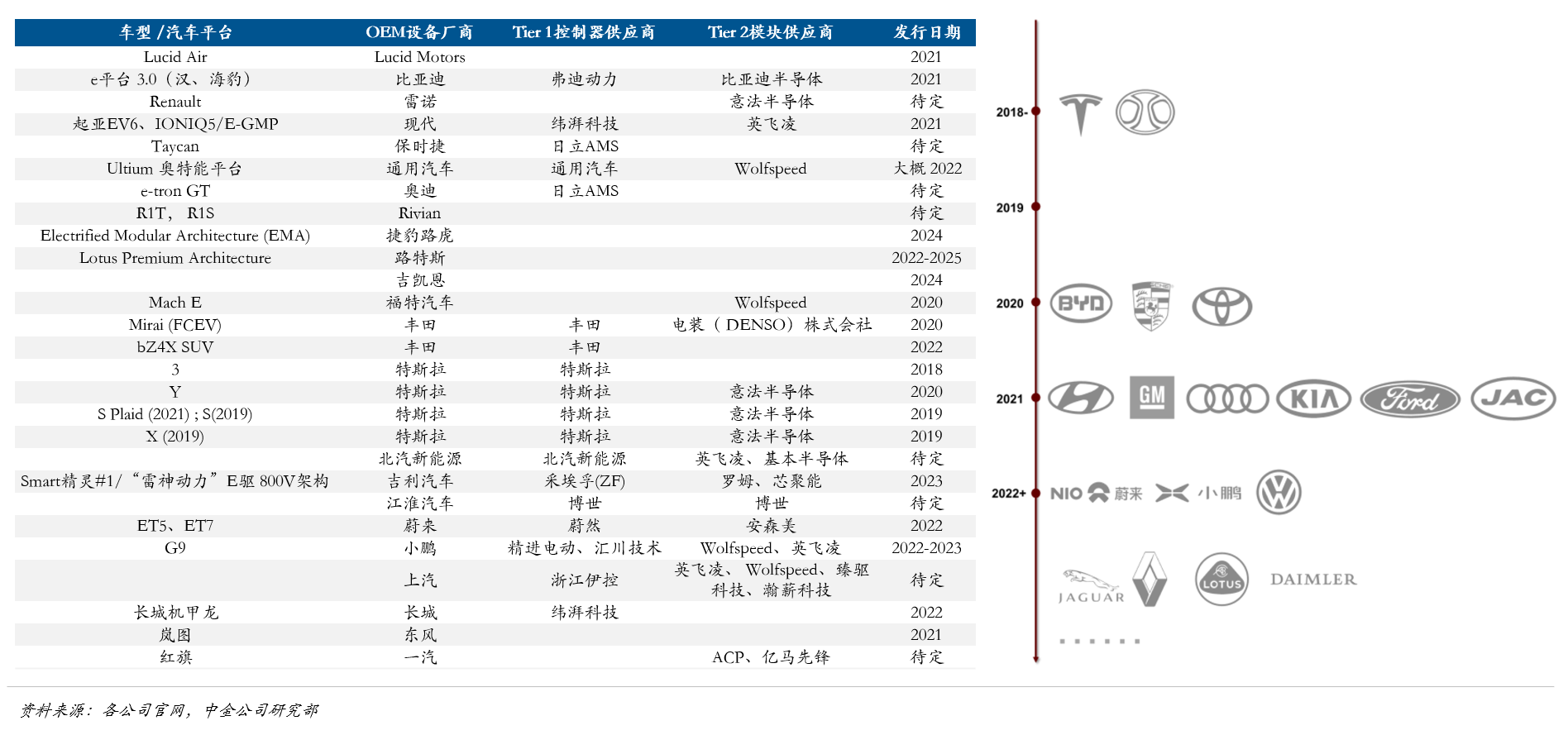
Models Equipped with SiC Main Inverters
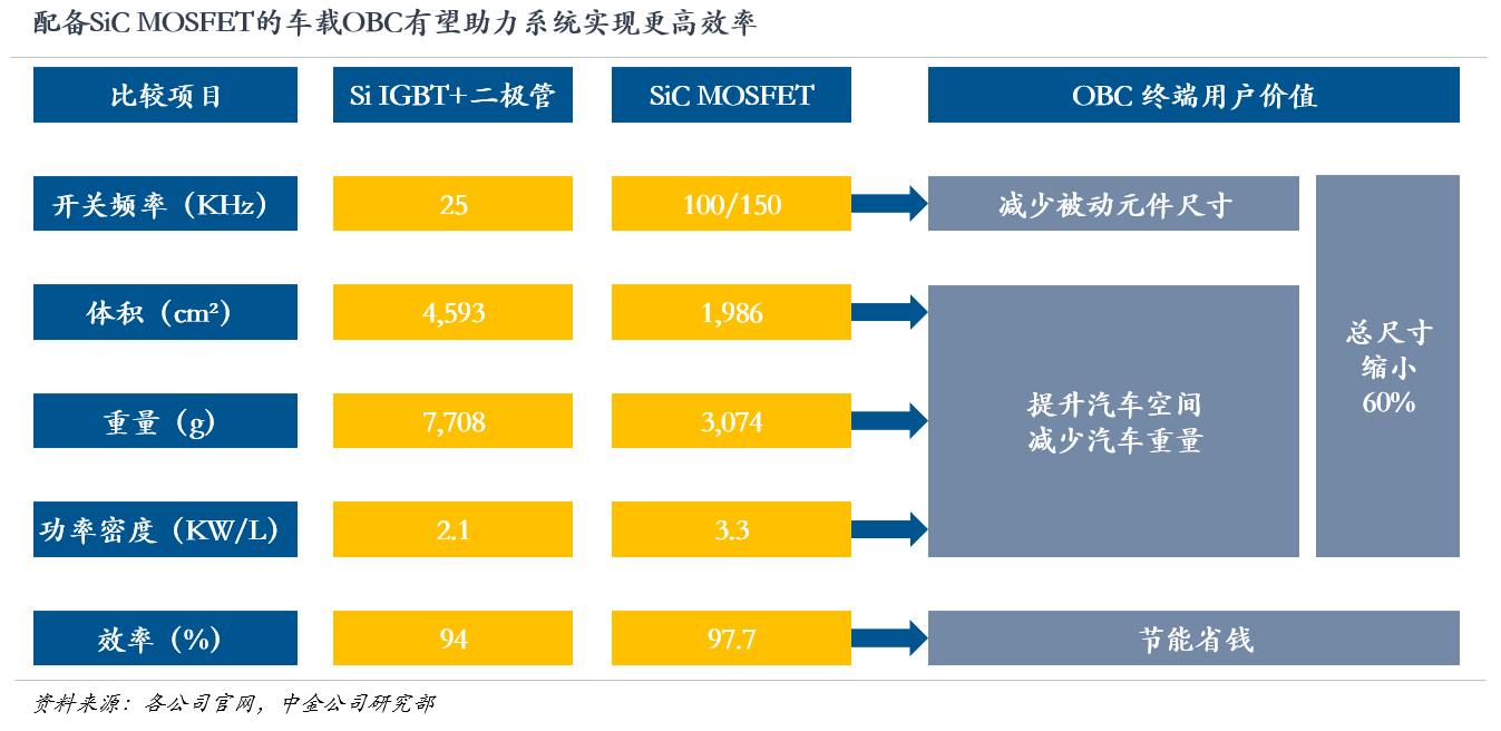
(2) New Energy Vehicle OBC
(3) New Energy Vehicle Charging Piles

3. Photovoltaic
In recent years, due to the overall downward trend in grid-connected electricity prices, photovoltaic inverters need to continuously improve operating efficiency and reduce the system cost per kilowatt-hour. Photovoltaic inverters equipped with silicon carbide devices are expected to meet the above requirements due to their excellent physical properties and become widely used in photovoltaic inverter applications.
Photovoltaic inverters operate by switching the polarity of the DC input current to approximate AC output. To improve efficiency, operating voltage, and power capacity, inverters need to balance switching frequency. According to data from Zhongshang Information Network, in photovoltaic power generation, traditional inverters based on silicon-based devices account for about 10% of the overall cost, but generate a large amount of system energy loss. According to data from the China Automotive Industry Information Network, photovoltaic inverters equipped with SiC MOSFETs or related power modules can increase the conversion efficiency from 96% to over 99%, reduce energy loss by more than 50%, and extend the service life by 50 times, which is conducive to reducing the system size, improving power density, and reducing production costs. Because power conversion efficiency is directly related to switching frequency, silicon carbide can handle higher voltages than silicon and ensure the ultra-high conversion frequency required for conversion efficiency, making it more suitable for photovoltaic power generation.
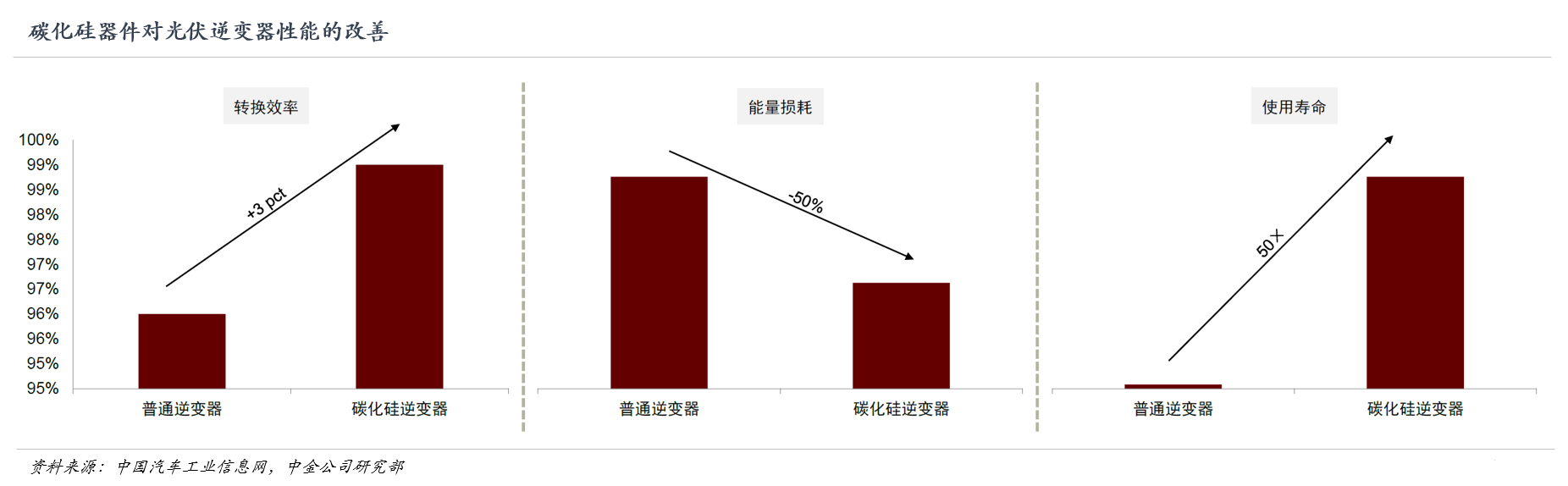
The operating characteristics of SiC in high-frequency fields also significantly reduce the size and weight of photovoltaic inverters equipped with SiC devices, increasing the possibility and convenience of installation in relatively harsh environments, and reducing installation and maintenance costs.
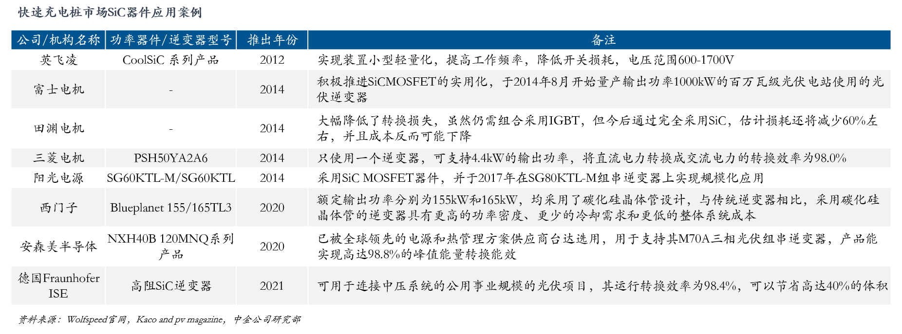
Infineon launched its first CoolSiC series devices in 2012, followed by Fuji Electric, Mitsubishi Electric, Siemens, and other manufacturers, who also launched their own silicon carbide power devices/inverters to improve energy conversion efficiency. In 2021, the Fraunhofer Institute for Solar Energy Systems (Fraunhofer ISE), one of the world's three major renewable energy research institutions, developed a "high-impedance SiC inverter" to provide a medium-voltage system connection solution for utility-scale photovoltaic projects.
Sungrow Power Supply started using SiC diodes in 30KW models in 2014 and achieved the use of SiC modules (80KW models) in 2017. Currently, silicon carbide products are widely used in Sungrow Power Supply products, replacing small and medium-sized inverters.
4. Rail Transit
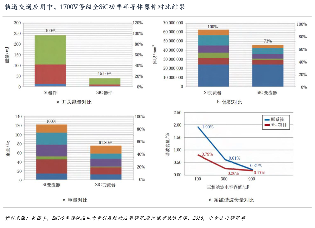
The characteristics of silicon carbide MOSFETs, suitable for high-voltage and high-temperature environments, make them promising for use in rail transit traction inverters. Locomotives equipped with SiC traction inverters not only reduce the number of components but also significantly decrease the total energy consumption of the onboard system. As shown in the figure on the right, using SiC power devices in a 1700V rail transit traction inverter reduces switching losses by approximately 84%, inverter volume by 27%, weight by approximately 38%, and improves system harmonic content, resulting in a significant improvement in system performance.
Specifically, the advantages of using silicon carbide in rail transit traction inverters include: (1) Improved size and weight, enhancing overall system performance. The significantly reduced switching losses of SiC power devices reduce heat generation in the power module, lowering the requirements for the power module heat sink and the entire inverter cooling system, resulting in reduced size and weight; in addition, power devices can switch at higher frequencies, reducing the size and weight of passive components such as transformers, capacitors, and inductors in the circuit. The improved overall size and weight of the inverter will benefit vehicle weight management and equipment layout, improving overall vehicle performance; (2) Improved system harmonics, increasing system efficiency. The reduced power consumption and increased switching frequency of SiC power devices will reduce system harmonic currents, thereby reducing harmonic interference to the power grid and improving system efficiency. The locomotive can also implement electric braking over a wider speed range, feeding back more electric braking energy to the grid.

5. Industrial Power Supplies
Content Source: Original by China Zhongji Investment. This report is for internal learning and research use only within China Zhongji Investment. All cited or referenced materials are noted. If there are any copyright issues, please contact us through the WeChat official account. The content of this report does not constitute investment advice to anyone, and the accuracy of the report content is not guaranteed. No unit may use the content of the report as evidence or basis for litigation, arbitration, or media citation, nor may it be used for profit or any other unauthorized purpose. If you need to cite, publish, or reprint this report, you must indicate the source and must not make any citation, deletion, or modification that contradicts the original meaning.
